

赫狄通納米
主營產(chǎn)品: 納米材料
基于285nm氧化層硅基底的CVD雙層石墨烯薄膜(1*1cm-4片裝)
價(jià)格
訂貨量(件)
¥4650.00
≥1
店鋪主推品 熱銷潛力款
ῡ῟ῥῡῠῦῢῠῢ῟ῧ
在線客服
生產(chǎn)廠商:Graphene Supermarket
產(chǎn)品信息

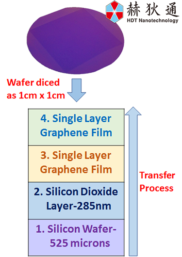
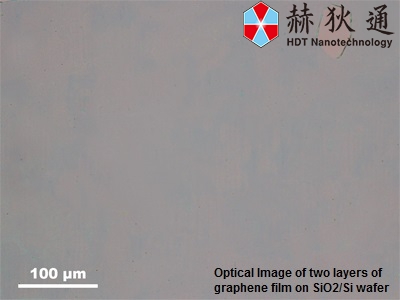
Two layers of single layer CVD graphene films are transferred onto 285 nm p-doped SiO2/Si wafer
Size: 1cmx1cm; 4 pack
Each graphene film is transferred consecutively onto the wafer
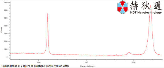
The thickness and quality of our graphene film is controlled by Raman Spectroscopy
The graphene coverage of this product is about 98%
The graphene film is continuous, with minor holes and organic residues
Each graphene film is predominantly single layer (more than 95%) with occasional small multilayer islands (less than 5% bi-layers)
Each graphene film is polycrystalline, i.e. it consists of grains with different crystallographic orientation
There is no A-B stacking order. The graphene films are randomly oriented with respect to each other
Sheet Resistance: 215-700 Ω/square
Oxide Thickness: 285 nm
Color: Violet
Wafer thickness: 525 micron
Resistivity: 0.001-0.005 ohm-cm
Type/Dopant: P/Boron
Orientation: <100>
Front Surface: Polished
Back Surface: Etched
Graphene electronics and transistors
Conductive coatings
Aerospace industry applications
Support for metallic catalysts
Microactuators
MEMS and NEMS
Chemical and biosensors
Multifunctional materials based on graphene
Graphene Research


采購數(shù)量不能為空
聯(lián)系信息不能為空

驗(yàn)證碼不正確