

赫狄通納米
主營產(chǎn)品: 納米材料
N型摻雜硅基底單層石墨烯(2.5cm*2.5cm)
價格
訂貨量(件)
¥5950.00
≥1
店鋪主推品 熱銷潛力款
祺祷祸祺祻祲祵祻祵祷祹
在線客服
生產(chǎn)廠商:Graphene Platform (Japan)
產(chǎn)品信息
Material : Single crystal silicon (CZ)
Orientation : ???100)
Type/Dopant : n/phosphoric
Resistivity : <50 ohm-cm
Wafer Size : 4 inch (100mm +/- 0.5 mm)
Thickness : 525 micron +/- 25 micron
Oxide Thickness: 1000aa (100nm)
Front Surface: Polished
(Representative Value)

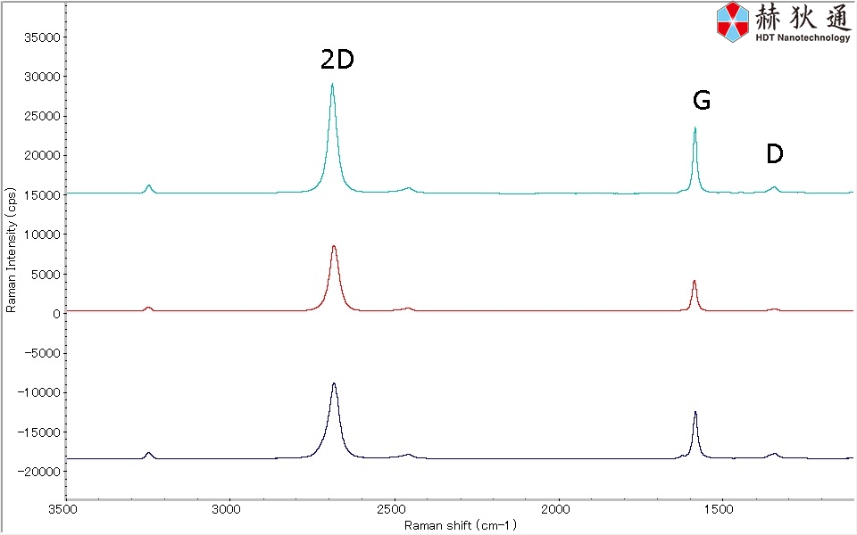
1. Raman spectroscopy is used to check the presence of a D peak in graphene samples. If a D peak is present, then this can indicate defects in the sample, such as cracks or flaking.
2. The ratio of the heights of the 2D peak and the G peak indicate the number of graphene layers.
2D>G : Single-layer
2D=G : Double layer
2D<G : more than triple layer
3. 3 measurements for every sample are taken and presented on the same graph.
采購數(shù)量不能為空
聯(lián)系信息不能為空

驗證碼不正確